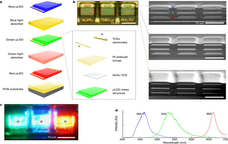
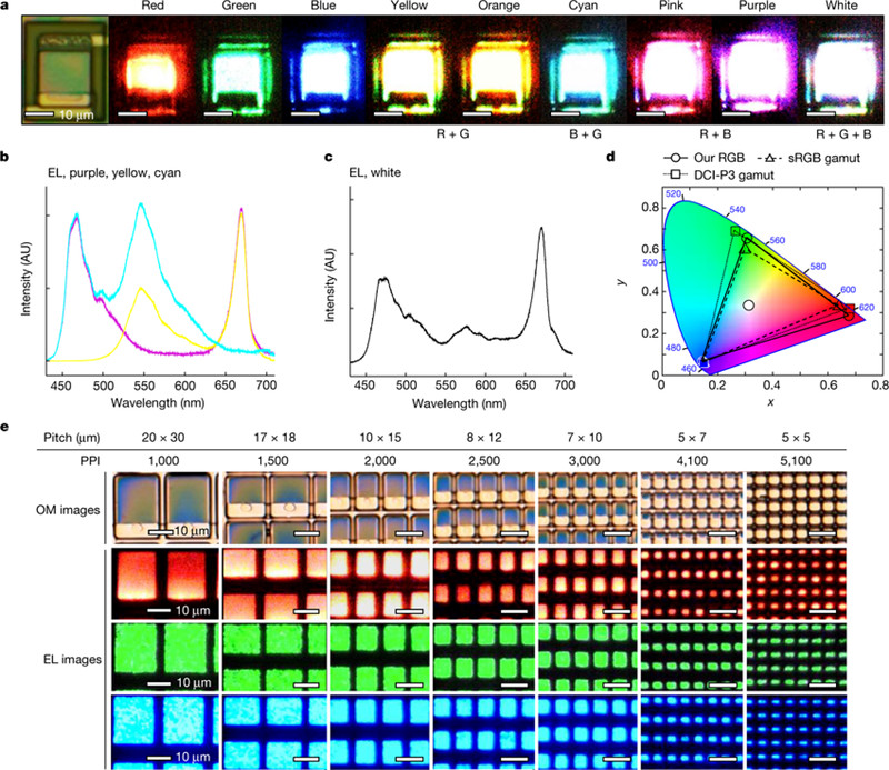
According to news on 3th February, a research team led by MIT recently announced in Nature magazine that the team has developed a full-color vertical stacked structure Micro LED with an array density of up to 5100 PPI and a size of only 4 μm. It is claimed to be the Micro LED with the highest array density and smallest size currently known.

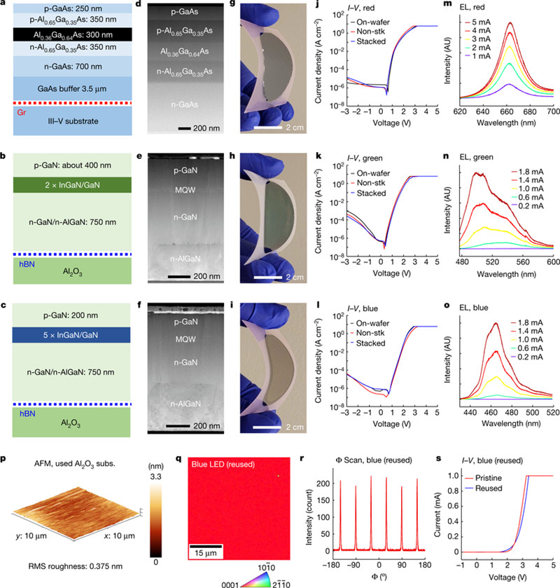
According to reports, in order to achieve high resolution and tiny size Micro LED, researchers used 2D materials based layer transfer (2DLT) technology.


This technology allows the growth of nearly submicron-thick RGB LEDs on two-dimensional material-coated substrates through fabrication processes such as remote epitaxy or van der Waals epitaxy growth, mechanical release, and stacking LEDs.
The researchers specifically pointed out that the stacking structure height of only 9μm is the key to creating high array density Micro LED.
The research team also demonstrated in the paper the vertical integration of blue Micro LED and silicon film transistors, which is suitable for AM active matrix drive applications. The research team stated that this research provides a new route for manufacturing full-color Micro LED displays for AR/VR, and also provides a common platform for a wider range of three-dimensional integrated devices.
All image source "Nature" magazine.
This article link
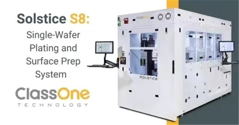
ClassOne Technology, a well-known equipment supplier for semiconductor electroplating and surface treatment in the United States, announced that it will provide a single crystal source electroplating system Solstice® S8 to a Micro LED manufacturer. It is reported that these new systems will be installed in the customer's new manufacturing base in Asia for the mass production of Micro LED.

Picture source: ClassOne Technology
ClassOne introduced that the Solstice® S8 system uses its proprietary GoldPro electroplating reactor, which can improve production efficiency and speed and reduce equipment costs. In addition, the Solstice® S8 system utilizes ClassOne's unique fluid motion profile technology to provide high plating rates and leading plating feature uniformity. ClassOne expects the Solstice® S8 system to begin shipping and installation in the second quarter of this year.
ClassOne stated that this order proves that the functionality of the Solstice platform is the key for customers to accelerate the preparation of Micro LED products for launch, and further verifies that ClassOne has leading single-wafer processing capabilities and technology status in the Micro LED field.
According to the data, ClassOne Technology is headquartered in Kalispell, Montana, USA. It can provide various electroplating and wet processing systems for optoelectronics, power, 5G, Micro LED, MEMS and other application markets.
In April last year, ClassOne supplied the Solstice® S4 single-wafer electroplating system to Micro LED microdisplay start-up Raxium to help it develop Micro LED microdisplays for AR/VR and promote product mass production.
Post time: Nov-09-2023

